Next: Alpha Decay Up: One-Dimensional Wave Mechanics Previous: WKB Approximation
 ,
which is directed such that it accelerates electrons away from the surface. We have
already seen (in Section 4.1.2) that electrons just below the surface
of a metal can be regarded as being in a potential well of depth
,
which is directed such that it accelerates electrons away from the surface. We have
already seen (in Section 4.1.2) that electrons just below the surface
of a metal can be regarded as being in a potential well of depth  ,
where is called the workfunction of the surface. Adopting a simple
one-dimensional treatment of the problem, let the metal lie at
,
where is called the workfunction of the surface. Adopting a simple
one-dimensional treatment of the problem, let the metal lie at  , and
the surface at
, and
the surface at  . Now, the applied electric field is shielded from the
interior of the metal. (See Section 2.1.12.) Hence, the energy,
. Now, the applied electric field is shielded from the
interior of the metal. (See Section 2.1.12.) Hence, the energy,  , say, of an electron just below the
surface is unaffected by the field.
In the absence of the electric field, the potential
barrier just above the surface is simply
, say, of an electron just below the
surface is unaffected by the field.
In the absence of the electric field, the potential
barrier just above the surface is simply  . The electric field
modifies this to
. The electric field
modifies this to
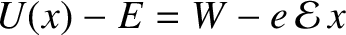 , where
  is the magnitude of the electron charge. The potential barrier is
sketched in Figure 4.11.
is the magnitude of the electron charge. The potential barrier is
sketched in Figure 4.11.
![\includegraphics[width=0.85\textwidth]{Chapter05/fig11_12.eps}](img3208.png) |
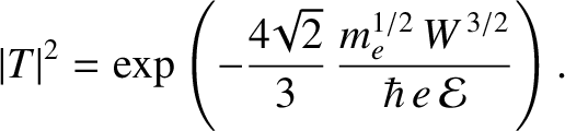
It can be seen, from Figure 4.11, that an electron just below the surface of the
metal is confined by a triangular potential barrier that extends from  to
to  ,
where
,
where 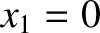 and
and
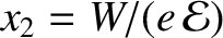 . Making use of the
WKB approximation (see Section 4.3.4), the probability of such an
electron tunneling through the barrier, and consequently being emitted from the surface,
is
. Making use of the
WKB approximation (see Section 4.3.4), the probability of such an
electron tunneling through the barrier, and consequently being emitted from the surface,
is
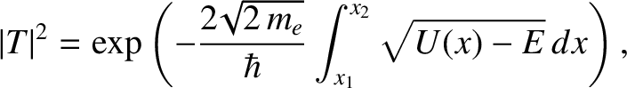 |
(4.142) |
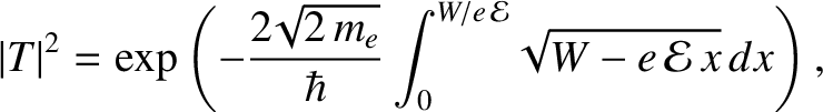 |
(4.143) |
 is the electron mass.
This reduces to
is the electron mass.
This reduces to
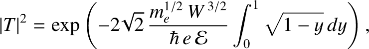 |
(4.144) |
The cold emission of electrons from a metal surface is the basis of an important device known as a scanning tunneling microscope, or an STM. An STM consists of a very sharp conducting probe that is scanned over the surface of a metal (or any other solid conducting medium). A large voltage difference is applied between the probe and the surface. Now, the surface electric field-strength immediately below the probe tip is proportional to the applied potential difference, and inversely proportional to the spacing between the tip and the surface. Electrons tunneling between the surface and the probe tip give rise to a weak electric current. The magnitude of this current is proportional to the tunneling probability, (4.145). It follows that the current is an extremely sensitive function of the surface electric field-strength, and, hence, of the spacing between the tip and the surface (assuming that the potential difference is held constant). An STM can, thus, be used to construct a very accurate contour map of the surface under investigation. In fact, STMs are capable of achieving sufficient resolution to image individual atoms.